TM 55-4920-401-13&P
the reference voltage,
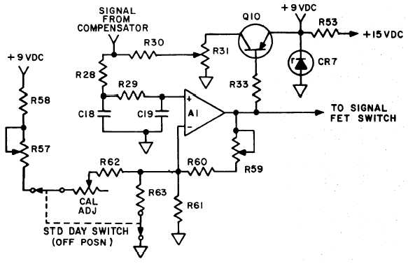
Figure 1-14. Temperature Indicator Amplifier Circuit.
1. The input signal is filtered by an R-C
network consisting of R28, C18, R29, and C19 (fig.
1-14). A voltage divider incorporating a poten-
tiometer (R31) makes it possible to adjust the indi-
cator so it will drift upscale, downscale, or remain
constant when the input is open. The voltage di-
vider supply (9 vdc) is controlled by Q10 which in
turn is driven by the output of amplifier Al. Q10
limits the voltage on the filter capacitors when the
potentiometer is adjusted for upscale drift.
2. The input signal is applied to the non-
inverting input of amplifier Al. A full-scale signal
is amplified to approximately 8.8 vdc. Applied to the
inverting input is the signal from a zero adjust cir-
cuit that has the configuration shown in figure 1-14
when the STD DAY switch is off. The zero adjust
circuit balances out the fixed compensator output
and amplifier offset voltages. R59 controls the gain
of the amplifier and calibrates the A/D converter at
the high end of the range.
(b) Reference Voltage Divider. The pre-
cision reference voltage divider consisting of re-
sistors R46-R52 is shown in figure 1-15. Transistors
Q11-Q15 ground different points of the divider dur-
ing the reference integration period and “shape”
generating a reference volt-
age curve that closely approximates the input sig-
nal curve. A transistor turns on when the cathode of
one of biasing zener diodes CR1-CR5 (2.6v) goes to
logic 0. The biasing circuits are controlled by flip-
flops on the temperature A/D converter board. Note
in figure 1-15 that all transistors are off during ref-
erence count 0-99. Transistor Q14 turns on during
counts 100-299, etc. The STD DAY switch grounds
the gate of Q17 in OFF position and turns Q17 on.
(3) Temperature Signal Circuits. The fol-
lowing subparagraphs explain all temperature
input signal circuitry except the standard day cir-
cuitry. Figures 1-16 and 1-17 show the temperature
input circuits. No attempt has been made to show
the circuits in detail, but merely to show the course
of each signal path so that a circuit can be traced
easily when troubleshooting. A single broken line is
shown for each path, whereas in reality, a circuit
contains two leads and passes through two sets of
switch poles and two sets of switch contacts. Cop-
per-constantan thermocouple wire is used to wire
the thermocouple input circuits because it is easier
to solder and its thermal characteristics are identi-
cal to chromel-alumel wire at normal ambient tem-
peratures.
1-13