TM 55-4920-401-13&P
Figure 1-7. Typical Reference Voltage Shaping.
(d) Comparator. The output of the inte-
grator is applied to the noninverting (+) input of
the comparator (fig. 1-8). The output of the com-
parator swings to 0 vdc when a positive voltage is
applied to the integrator and to +5 vdc when a
negative voltage is applied to the integrator.
(e) FET Switch Control. Three junction
field-effect transistors (Q5-Q7, fig. 1-9) control the
input to the integrator. The output of the signal am-
plifier is controlled by Q5, the positive reference
voltage is controlled by Q6, and the negative refer-
ence voltage is controlled by Q7. The FET control-
ling signals are the comparator output and a deco-
ded signal, INTEGRATE SIGNAL, which is low
during its active period.
1. At the beginning of the signal integra-
tion period, INTEGRATE SIGNAL goes to logic 0,
turning Q1 on and Q2 off. The values of R1 and R3
are such that Q2 remains off even if the comparator
output goes to 0 vdc. Q3 and Q4 turns on. Plus 15
vdc from Q3 turns on Q5. Minus 15 vdc from Q4
turns off Q6. Minus 15 vdc also turns off Q7.
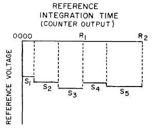
2. At the beginning of the reference inte-
gration period, INTEGRATE SIGNAL goes to logic
1, turning off Q1, Q3, and Q5. At the same time, Q2
is enabled so that 0 vdc from the comparator can
turn on Q2. If the input signal is positive, the com-
parator will have a 0 vdc output at the end of the
signal integration period and will turn on Q2. Logic
1 voltage from Q2 will turn on both Q4 and Q7. Q4
holds Q6 off, keeping the positive reference voltage
off. The negative reference voltage is turned on by
Q7. If the input signal to the A/D converter is nega-
tive, then the output of the comparator will be +5
vdc at the end of the signal integration period. Q2
will turn off, reversing the sequence for a negative
input signal. The positive reference voltage will be
turned on and the negative reference will be turned
off.
3. The period from the conclusion of the
reference integration period to the beginning of the
subsequent signal integration period is referred to
as the oscillate period. During the oscillate period,
the integrator output it kept close to 0 vdc by rap-
idly and alternately turning on and off the positive
and negative reference voltage FET’s. This high fre-
quency oscillation ends when INTEGRATE SIGNAL
goes low.
( f ) G e n e r a t i o n o f T r a n s f e r - t o - M e m o-
ry. At the conclusion of the reference integration
period, transfer-to-memory transfers the contents
of the counter-latch-decoder counters on the dis-
play-counter board into the latches, updating the
n u m e r i c a l d i s p l a y . T r a n s f e r - t o - m e m o r y is
1-8