TM 55-4920-401-13&P
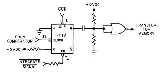
Figure 1-10. Circuitry That Generates Transfer-to-Memory.
generated when FF1A (fig. 1-10) is cleared. FF1A
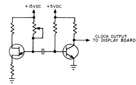
(g) Clock Oscillator. The clock oscillator
may be cleared in one of two ways: (1) when it is
(fig. 1-11) provides the time base for the signal and
clocked by the comparator at the conclusion of the
reference integration periods. It consists of a relax-
reference integration period of an in-range signal,
ation oscillator and pulse amplifier transistor. Os-
and (2) by the out-of-range signal (OOR) when the
cillator frequency is determined by the type of input
input signal is detected to be negative or positive
signal and indicator range.
out-of-range. Positive out-of-range signals are de-
(h) Display and Counter Board. T h e
tected by out-of-range decoding (fig. 1-3) and nega-
tive out-of-range signals cause the comparator to
clock oscillator signal (CLOCK) from each A/D con-
verter is applied to a string of counter-latch-decoder
set FF2A at the conclusion of the signal integration
(CLD) integrated circuits (fig. 1-12) on the display
period. FF1A (fig. 1-10) is preset at the beginning of
the signal integration period.
and counter board. The counter-latch-decoders drive
resistor devices (RD’s) which in turn drive the dis-
Figure 1-11.
Clock oscillator.
1-10