TM 55-4920-401-13&P
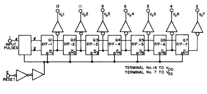
4 . S e v e n - S t a g e B i n a r y C o u n t e r
is reset to “zero” by a high level on the reset input.
(CD4024AE). This counter consists of an input
Each counter stage is a static master-slave flip-flop.
pulse shaping circuit, reset line driver circuitry, and
The counter state is advanced one count on the
seven binary counter stages (fig. 1-30). The counter
negative-going transition of each input pulse.
Figure 1-30. Functional Diagram of 7-Stage Binary Counter.
5. Seven-Segment LED Display (5082-
7650). This is a large (0.43”) red, common anode,
seven-segment display with left-hand decimal
point. Figure. 1-31 shows the schematic and the con-
nection to drive circuitry. Table 1-4 lists pin func-
tions.
6. Counter-Latch-Decoder (MC4350L).
This device (fig. 1-32) combines the functions of an
NBCD counter, four-bit latch, and a seven-segment
decoder/driver. The counter advances on input. The
serial output is high driving the ninth count, allow-
ing synchronous or asynchronous counter operation
when used in conjunction with the enable input and
some external gating. The counter reset places the
counter in a non-NBCD state, turning off the output
driver transistors when transferred through the
latch and decoded. This feature gives automatic
suppression of leading zeros in the display. The
latch section admits information while the strobe is
high and latches the data on the negative edge of
the strobe. A lamp blanking input is provided for in-
tensity modulation, A lamp test feature is also
available. Circuit operation is summarized in table
1-5.
1-31


